Capture the performance, power, and economic benefits of custom silicon with a partner that connects architecture, proven technology, manufacturing, supply and volume execution from the start.
Marvell is a custom silicon design partner for leading cloud, AI, and data center companies developing differentiated architectures. Each custom silicon program is structured around the customer’s architecture, internal capabilities, workload priorities, and platform roadmap. Programs can combine customer-developed technology, Marvell IP, third-party IP, open standards, chiplets, companion devices, or complete custom ASIC designs.
The same technology foundation opens the door to a broad range of custom products, from custom AI accelerators and XPUs to co-processors, network interfaces, memory, security, scale-up fabrics, and entirely new architectures built around customer requirements.
From workload priorities to volume deployment
A coordinated engagement connects the critical decisions from early requirements through production, helping reduce execution risk and maintain alignment as the program moves toward volume.

Workload, system, software, performance, power, deployment, and roadmap priorities agreed before the architecture is set.

Compute, memory, connectivity, packaging, power, and supply evaluated as one system - validated with models, test chips, and silicon data.

Architecture, IP, design, packaging, software, test, and operations kept aligned through verification, first silicon, and bring-up.

Qualification, yield, manufacturing readiness, capacity, and volume ramp - continuing into production optimization and future generations.
The Marvell custom technology portfolio addresses the areas that increasingly determine AI platform performance, power, integration, and scale. The technologies can be used individually, customized around the customer architecture, or combined within a broader custom ASIC program.
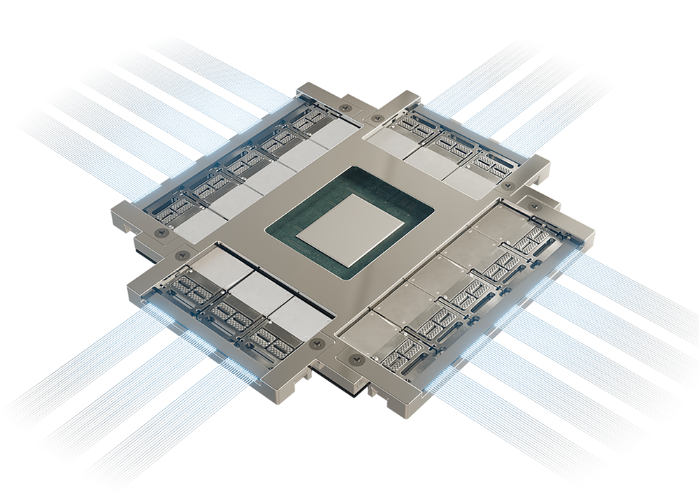
Advanced packaging integrates compute dies, HBM, I/O chiplets, power delivery, and high-speed connectivity into one deployable system.
Marvell develops the package alongside the silicon architecture. Workload requirements, chiplet design and XPU partitioning, memory capacity, rack topology, and power constraints inform how functions are distributed across the package.
Die-to-die connectivity, HBM placement, substrates, package escape, power delivery, cooling, test, yield, and manufacturing are then evaluated as one architecture.
System-level co-design across compute, memory, connectivity, power, thermals, and manufacturing
Modular packaging technologies that can be reused across platform generations
Support for interposers, silicon bridges, advanced substrates, custom HBM, package-integrated power, copper, and optics
Leading foundry, bridge-based, and OSAT manufacturing paths
Early alignment across foundry, memory, substrate, packaging, power, and optical partners
The Marvell roadmap extends from current 2.5D multi-die systems to vertically stacked silicon, embedded package functions, and package-integrated connectivity.
The result is a path to more compute, memory, and I/O without allowing package complexity, power delivery, thermals, or manufacturing readiness to limit deployment.
AI platforms depend on high-speed data movement between compute, memory, hosts, switches, racks, data centers, and regions.
Each connection presents a different balance of bandwidth, reach, power, latency, signal loss, protocol requirements, and silicon area. Marvell develops SerDes across these electrical and optical connectivity domains and optimizes each implementation around the channel, package, process technology, and system architecture.
Co-optimization of lane rate, reach, power, latency, signal integrity, and silicon area
Direct engineering support for channel definition, modeling, integration, and validation
Technology roadmaps aligned with increasing AI bandwidth requirements
Silicon and production experience from implementation in switches, retimers, optical devices, and custom platforms
This breadth allows customers to coordinate connectivity across the complete infrastructure instead of managing separate technology strategies for each interface.
The result is bandwidth that scales with the platform while maintaining the power, reach, and reliability required for deployment.
Chiplet design allows compute, memory, and I/O to scale independently. Die-to-die interconnect determines how efficiently those chiplets operate as one accelerator.
Marvell D2D IP is designed for high bandwidth density with limited power, latency, die edge, and internal silicon overhead. The interface can be optimized with the compute architecture, custom HBM, I/O chiplets, process technology, and advanced package.
Compact, high-density connectivity between compute, memory, and I/O dies
Simultaneous bidirectional signaling that increases the bandwidth available from a given interface area
A complete subsystem spanning the physical interface, adapters, bridges, link management, error correction, replay, redundancy, and lane repair
Support across multiple process nodes and package technologies
Standards-based and custom interface options based on the needs of the architecture
Open standards provide portability where broad ecosystem compatibility is required. Custom D2D provides additional optimization where power, latency, area, or bandwidth density has a greater effect on the complete platform.
The result is greater flexibility in how the XPU is partitioned, with more silicon available for compute, memory, and differentiated customer logic.
HBM provides the bandwidth required by advanced AI accelerators. The conventional interface can also consume substantial compute-die area, package routing, power, and thermal headroom.
Marvell custom HBM replaces the large conventional JEDEC HBM interface on the XPU with an optimized D2D connection to a customized HBM base die. Selected interface, control, management, and telemetry functions can be placed on the base die rather than on the leading-edge compute silicon.
Co-design of the XPU interface, controller, D2D link, base die, and package
Placement of memory-related functions on the silicon best suited to perform them
Coordination across reliability, telemetry, firmware, verification, power, and thermal requirements
Integration with established HBM stacks from the customer’s selected memory supplier
Flexible models for customer-procured memory or a more complete Marvell-managed solution
A roadmap aligned with future memory, packaging, and XPU generations
The custom base die becomes part of the accelerator architecture rather than a fixed memory component.
The result is more flexibility in how compute area, memory capacity, interface power, and package resources are allocated across the platform.
On-chip SRAM supplies activations, intermediate results, buffers, tables, queues, and control data directly to the compute cores.
General-purpose memory compilers may not provide the required balance of bandwidth, capacity, power, timing, port structure, and physical dimensions. Marvell develops custom SRAM around the workload, compute architecture, and floorplan.
Custom bitcells, circuits, macro architectures, compiler technology, and physical-design methods
Optimization across width, depth, capacity, ports, interfaces, access timing, clocking, and power states
Macro dimensions and aspect ratios tailored to the XPU floorplan
Redundancy, repair, reliability, and customer-specific functions
High-bandwidth memory architectures designed to keep parallel compute resources active
Co-optimization with HBM, D2D, packaging, and the complete memory hierarchy
Custom memory can reduce the number of general-purpose macros, simplify routing and floor-planning, and use leading-edge silicon more efficiently.
The result is more local bandwidth with less area and power devoted to memory overhead.

Custom silicon is a multi-year infrastructure commitment with implications for performance, economics, capacity, and roadmap control. Marvell helps AI, cloud, and infrastructure companies make that commitment with greater confidence and carry it through to volume deployment.
Earlier visibility into constraints: Memory, connectivity, power, thermals, package feasibility, test, yield, and capacity are evaluated while the architecture is still flexible.
Proven technology choices: Hardware-proven IP, test chips, product silicon, models, and validation environments support critical design decisions.
Clear program ownership: Responsibilities, interfaces, milestones, and dependencies are defined across customer, Marvell, and ecosystem teams.
Manufacturing aligned from the start: Foundry, memory, substrate, packaging, assembly, test, qualification, and capacity planning are connected to the design process.
Continuity across generations: Reusable IP, interfaces, chiplet boundaries, package strategies, and manufacturing paths support future platforms.

Custom silicon is purpose-built semiconductor chip designed around specific workload, system, power, and infrastructure requirements. For AI infrastructure, it can optimize compute, memory, connectivity, packaging, and other system functions around the needs of a target application.
Custom silicon can improve TCO by optimizing performance, power, memory, connectivity, and silicon resources around the target workload. Marvell helps evaluate these tradeoffs alongside development cost, manufacturing, packaging, utilization, and deployment scale to support stronger platform-level economics.
The technology portfolio can be applied across a broad range of custom silicon, including AI accelerators, co-processors, network interfaces, memory, security devices, and scale-up fabrics. These are representative categories rather than the limits of what can be developed around a customer-defined architecture.
Engagements can range from selected IP and defined design responsibilities to chiplets, companion silicon, implementation support, or a complete custom silicon program. The model is structured around the customer’s architecture and internal capabilities.
Hardware-proven IP, test chips, product silicon, models, demonstrations, interface analysis, and validation environments provide evidence for key architecture and integration decisions before full implementation.
Marvell coordinates across wafers, memory, substrates, packaging, assembly, and test. Planning includes production ramp, capacity, supplier diversification, lifecycle support, and recovery requirements to support deployment at the required scale.
Custom silicon costs can include NRE, IP licensing, masks, wafers, packaging, HBM or other memory, assembly, test, qualification, and production. Marvell works with customers to evaluate these costs alongside volume, yield, capacity, performance, power, expected platform life and overall platform-level TCO.
Milestones, ownership boundaries, escalation paths, change controls, and dependencies are defined across customer, Marvell, and ecosystem teams. Technical commitments and commercial requirements remain aligned as the program progresses.
The engagement continues through yield improvement, lifecycle support, and planning for subsequent platform generations.
We believe better partnerships help to build better technologies. Let’s connect and see what we can design together!
We will be in touch with you soon!