By Andrew Yick, Technical Associate Vice President, Operations Engineering, Marvell
This article was first published in Photonic Integrated Circuits magazine.
The dominant challenge in modern AI infrastructure is not just the performance of a single accelerator but scaling up to thousands of accelerators (XPUs) in a cluster. Training and inference workloads now depend on an interconnect that can stitch these accelerators into a high-bandwidth, low-latency system, where performance is governed as much by the network as by the compute itself.
As these systems scale, physics asserts itself. Electrical links over copper hit a practical ceiling as routing density and channel loss collide, turning the loss bandwidth product into an impassable constraint. The choice is binary: either move electrical-to-optical conversion closer to the Application-Specific Integrated Circuit (ASIC) or surrender the link budget. Thus, to bypass this electrical wall, optics must migrate from the board edge and onto the ASIC package.
By Preet Virk, Senior Vice President and General Manager, Photonic Fabric Business Unit
Modern AI infrastructure is built around multi-rack systems where thousands to tens of thousands of accelerators operate as a single logical compute element. As agentic AI and Mixture of Experts (MoE) models accelerate AI adoption, they are driving unprecedented scale and communication demands across data center infrastructure. These systems are connected by scale-up and scale-out networks that must deliver high bandwidth, low latency and efficient power. As these networks extend across racks, maintaining that performance becomes a primary challenge.
As AI systems grow in complexity and scale, the network becomes the backbone of the compute system. Large-scale clusters require massive XPU-to-XPU communication, driving an evolution beyond legacy protocols like PCIe® to encompass UALink™ (Ultra Accelerator Link), ESUN (Ethernet scale-up networking) and NVLink.
Meeting these requirements demands a new approach to connectivity. Marvell provides a comprehensive AI connectivity portfolio spanning scale-up, scale-out, scale-across and DCI (data center interconnect) network architectures. For scale-up networking, Marvell delivers copper and optical interconnects connecting XPUs, switches and memory. Within the rack, Marvell copper solutions provide low-latency, power-efficient short-reach connectivity, while Marvell optical interconnects enable high-performance scaling beyond the rack. This enables XPUs to operate as a more efficient, unified system as scale-up domains expand.
By Jianping Jiang, Head of Product Marketing, CXL Switch, Marvell
The AI memory wall—the widening gap between the memory capacity and bandwidth AI infrastructure wants and the amount that conventional memory architectures can deliver—is accelerating at an alarming pace.
And the consequences are getting increasingly ominous for data center operators and their customers: idle XPUs, underutilized equipment, longer processing times, higher costs, and ultimately a lower return on investment. Meanwhile, memory—already second only to GPUs in datacenter semiconductor spend1—continues to soar in price.
The Marvell® StructeraTM S family of Compute Express Link (CXL) switches scale the memory wall by providing a pathway for adding terabytes of shareable memory to infrastructure and dynamically allocating bandwidth and capacity to boost utilization and application performance. CXL switches don’t just boost memory and memory capacity; they enable data center operators to use it more wisely too.
Structera S is the successor to the groundbreaking Apollo line of CXL switches developed by XConn Technologies, now part of Marvell. Structera S 20256 for PCIe Gen 5.0/CXL 2.0 (previously the XConn Apollo I) became the first commercially available CXL switch upon its release last year.
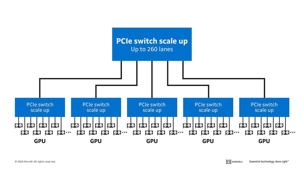
Marvell is expanding the family with Structera S 30260 for PCIe 6.0/CXL 3.x. Structera S 30260 features support for 16 or 32 CPUs or GPUs over 260 lanes with up to 48TB of shared memory and 4TB/second cumulative bandwidth. Marvell is showcasing Structera S 30260 in a live demonstration this week at OFC 2026 and plans on sampling to customers in 3Q 2026.
By Krishna Mallampati, Senior Director of Product Marketing, Data Center Switching, Marvell
Since its introduction in 2004, PCIe® has become the most popular interconnect for low-latency chip-to-chip connections. From its humble beginnings for fan-out interconnects, PCIe has been integrated into AI and cloud servers, JBOF storage systems, ADAS systems in automotive, industrial automation, PCs, and other platforms.
Scale-up AI servers—which can contain hundreds of processors spread over multiple racks—represent the next logical step for PCIe. Although far larger than today’s single chassis AI servers, scale-up servers demand the same thing from interconnect fabrics: coherent, low-latency links that enable fast, secure communication between components. PCIe’s status as a widely-used standard that evolves to meet customer demands further puts it in the forefront for scale-up.
Let’s explore the PCIe scale-up usage model and how these architectures will evolve.
PCIe Scale-up Usage Model
By Xi Wang, Senior Vice President and General Manager of the Connectivity Business Unit, Marvell
Marvell has become a founding member of the eXtra dense Pluggable Optics (XPO) Multi-Source Agreement (MSA), an industry initiative organized by Arista Networks to define a new optical transceiver form factor purpose-built for AI-scale infrastructure.
The XPO concept is designed to dramatically increase bandwidth density by enabling liquid cooling at the module level. XPO modules are substantially larger in size than octal small form factor pluggable (OFSP) modules commonly deployed in today’s data centers, but they deliver a step-function increase in performance. Each XPO module integrates 64 lanes operating at 200 Gbps, eight times more than current pluggable modules for a total of 12.8 Tbps of bandwidth per module.1
This leap in bandwidth is enabled in part by an integrated cold plate that can deliver up to 400W of cooling per module. The combination of larger modules, significantly higher lane counts, and liquid cooling delivers a four-fold increase in bandwidth density for switches across scale-up, scale-out or scale-across network architecture.