

This blog was originally posted in Semiconductor Engineering.
The semiconductor industry is the bedrock of modern technology, enabling everything from AI and cloud computing to electric vehicles. Yet, this critical sector is also one of the most resource-intensive globally, with a substantial dependency on water. A single fabrication plant can demand up to 10 million gallons of water daily, comparable to the consumption of a city with 300,000 residents. Much of this water is, of course, reused and recycled through sophisticated systems. This immense water usage, particularly the requirement for ultrapure water for processes like cleaning and etching, makes consistent access to high-quality water a non-negotiable for operational reliability and business continuity. The new insights report “Ripple Effects: Water Risk and Resilience Across the Semiconductor Value Chain” provides the first global baseline of water risk hotspots for the semiconductor sector, assessing water risks across 140 facilities across 89 water basins to inform future risk mitigation strategies.

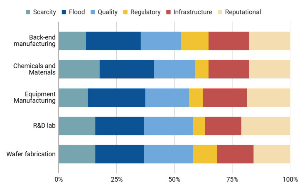
The analysis discusses how water risk can manifest itself as a financially material impact on business continuity by triggering idle time, recovery costs, and cascading delivery delays across global supply chains. S&P Global projects that by 2050, water-related risks could cost the world’s largest IT companies up to $24 billion annually. Crucially, the study identified flooding and reputational risks—such as strained relationships with local communities over water allocation—as the most significant immediate threats to the semiconductor value chain. These concerns are most acute in major hubs like Taiwan, South Korea, and parts of the U.S.

Global proportional distribution of water-related risks across the semiconductor value chain, broken down by value chain segment and risk type (Source: SEMI; Waterplan Water Risk Framework)
While the industry is frequently criticized for its water usage, only 16% of the analyzed sites are currently affected by water scarcity. However, this metric offers a false sense of security. As climate change intensifies, the frequency and severity of water-related disruptions are set to exceed the scope of existing contingency plans. The long-term projections show that over 40% of semiconductor facilities announced since 2021 are located in watersheds projected to face high or extremely high water stress between 2030 and 2040. This underscores the urgent need to integrate forward-looking risk modeling into new site planning to ensure long-term operational resilience.
Effective risk management is significantly hindered by the limited transparency surrounding supplier-level water data. While many companies perform water assessments for their direct operations, a comprehensive, industry-wide approach to supplier data and risk management is lacking. CDP data shows that 1 in 5 companies reported $77 billion under threat from supply chain water risks, yet only half of those companies engage with their suppliers on these issues. For semiconductor end users, these risks are often deep within multi-tiered networks, requiring engagement that goes well beyond Tier 1 suppliers.
To manage these complex risks, the report stresses the necessity of moving toward a contextual approach that includes localized assessments. Contextual water risks are inherently location-specific, dependent on local availability, quality, and infrastructure, as well as broader catchment-level dynamics, regulatory pressures, and community expectations. Several structured methodologies support this necessary shift from basic operational management to corporate water stewardship, including the Alliance for Water Stewardship (AWS) Standard, the TNFD’s LEAP framework, and the Science Based Targets for Nature (SBTN). This approach encourages companies to look beyond their own operations to safeguard regional water security.

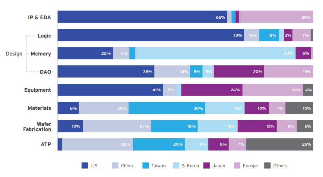
Semiconductor industry value added by activity and region, 2024. Value contributions are based on company revenues and headquarters location for IP (Intellectual Property) & EDA (Electronic Design Automation), design, manufacturing equipment, and raw materials. Wafer fabrication and ATP (Assembly, Testing & Packaging) are measured by installed capacity and the geographic location of production facilities. (Source: SEMI; SIA, adapted from IPnest, Wolfe Research, Gartner, SEMI, and BCG analysis).
Because water is a shared resource, collective action is essential to deliver the scale and urgency needed to tackle common challenges within catchments. The semiconductor value chain is deeply interconnected, with companies often sharing suppliers within the same water basins, creating a strategic opportunity for collaborative stewardship. The report encourages companies to scale their impact by moving beyond isolated efforts to form sector-wide and cross-sector partnerships—especially at the catchment level—through public-private engagement. This collaboration, which includes proactive engagement with policymakers and local utilities, is key to aligning on water management and stewardship practices to address shared water challenges and build collective trust.
Innovation and technology must play a central role in advancing water stewardship across the value chain. A major hurdle is the general undervaluation and mispricing of water, which perpetuates systemic underinvestment in water-focused technology. Despite this, leading semiconductor companies are deploying advanced solutions such as onsite recycling systems, real-time water monitoring, and utilizing alternative sources like municipal wastewater. Embracing AI-driven systems for scenario modeling and catchment-level risk forecasting further enhances adaptive capacity and resilience.
The “Ripple Effects” report makes it clear that water challenges affect every segment, demanding tailored response tactics and strategies. Foundries, with their large operational footprints, must prioritize sourcing reclaimed water and expanding onsite reuse, while chemical and materials suppliers must proactively manage rising regulatory risks around water quality contaminants.
The insights report also provides a practical roadmap for advancing corporate water stewardship, outlining progression from water risk assessment (Stage 1) to site-level action and collective engagement (Stage 2), and culminating in transparent validation and reporting (Stage 3). By following a structured water stewardship pathway, the semiconductor industry can build operational resilience and ensure a responsible future for the entire value chain.
To learn more, download the report or watch the webinar recording.
# # #
This blog contains forward-looking statements within the meaning of the federal securities laws that involve risks and uncertainties. Forward-looking statements include, without limitation, any statement that may predict, forecast, indicate or imply future events or achievements. Actual events or results may differ materially from those contemplated in this blog. Forward-looking statements are only predictions and are subject to risks, uncertainties and assumptions that are difficult to predict, including those described in the “Risk Factors” section of our Annual Reports on Form 10-K, Quarterly Reports on Form 10-Q and other documents filed by us from time to time with the SEC. Forward-looking statements speak only as of the date they are made. Readers are cautioned not to put undue reliance on forward-looking statements, and no person assumes any obligation to update or revise any such forward-looking statements, whether as a result of new information, future events or otherwise.
Tags: data centers, Semiconductor, ESG