By Michael Kanellos, Head of Influencer Relations, Marvell
The opportunity for custom silicon isn’t just getting larger – it’s becoming more diverse.
At the Custom AI Investor Event, Marvell executives outlined how the push to advance accelerated infrastructure is driving surging demand for custom silicon – reshaping the customer base, product categories and underlying technologies. (Here is a link to the recording and presentation slides.)
Data infrastructure spending is now slated to surpass $1 trillion by 20281 with the Marvell total addressable market (TAM) for data center semiconductors rising to $94 billion by then, 26% larger than the year before. Of that total, $55.4 billion revolves around custom devices for accelerated compute1. In fact, the forecast for every major product segment has risen in the past year, underscoring the growing momentum behind custom silicon.
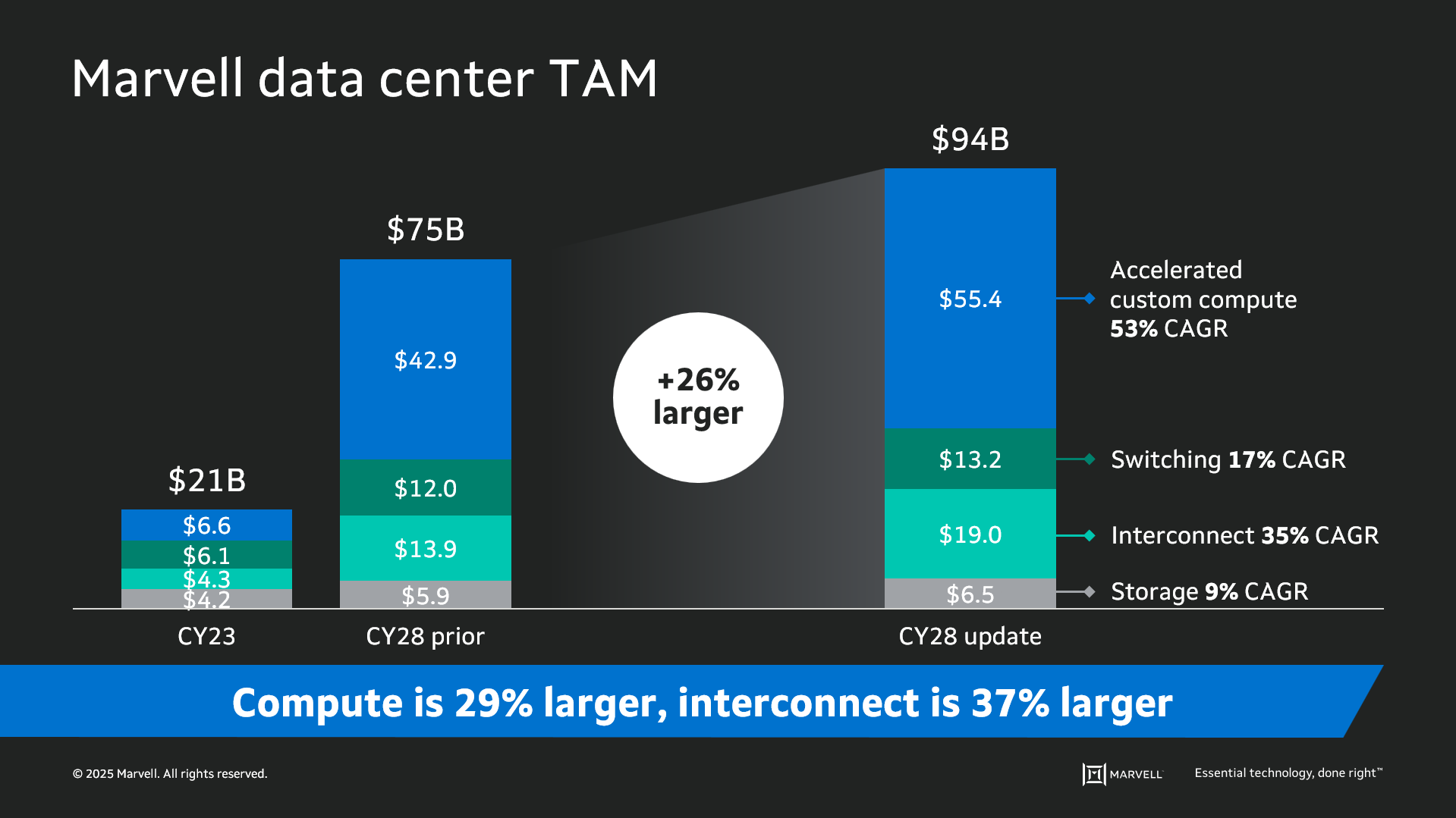
The deeper you go into the numbers, the more compelling the story becomes. The custom market is evolving into two distinct elements: the XPU segment, focused on optimized CPUs and accelerators, and the XPU attach segment that includes PCIe retimers, co-processors, CPO components, CXL controllers and other devices that serve to increase the utilization and performance of the entire system. Meanwhile, the TAM for custom XPUs is expected to reach $40.8 billion by 2028, growing at a 47% CAGR1.
By Nizar Rida, Vice President of Engineering and Country Manager, Marvell Canada
This blog first appeared in The Future Economy
AI has the potential to transform the way we live. But for AI to become sustainable and pervasive, we also have to transform our computing infrastructure.
The world’s existing technologies, simply put, weren’t designed for the data-intensive, highly parallel computing problems that AI serves up. As a result, AI clusters and data centers aren’t nearly as efficient or elegant as they could be: in many ways, it’s brute force computing. Power1 and water2 consumption in data centers are growing dramatically and many communities around the world are pushing back on plans to expand data infrastructure.3
Canada can and will play a leading role in overcoming these hurdles. Data center expansion is already underway. Data centers currently account for around 1GW, or 1%, of Canada’s electricity capacity. If all of the projects in review today get approved, that total could grow to 15GW, or enough to power 70% of the homes in the country.4
Like in other regions, data center operators are exploring ways to increase their use of renewables and nuclear in these new facilities along with ambient cooling to reduce their carbon footprint of their facilities. In Alberta, some companies are also exploring adding carbon capture to the design of data centers powered by natural gas. To date, carbon capture has not lived up to its promise.5 Most carbon capture experiments, however, have been coupled with large-scale industrial plants. It may be worth examining if carbon capture—combined with mineralization for long-term storage—can work on this smaller scale. If it does, the technology could be exported to other regions.
Fixing facilities, however, is only part of the equation. AI requires a fundamental overhaul in the systems and components that make up our networks.
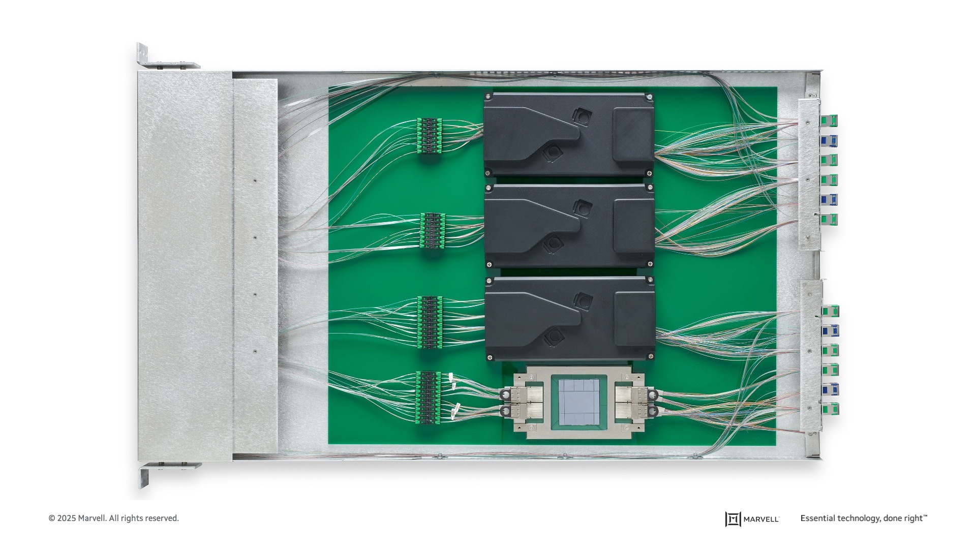
Above: The server of the future. The four AI processors connect to networks through four 6.4T light engines, the four smaller chips on the east-west side of the exposed processor. Coupling optical technology with the processor lowers power per bit while increasing bandwidth.
By Michael Kanellos, Head of Influencer Relations, Marvell
Bigger is better, right? Look at AI: the story swirls with superlatives.
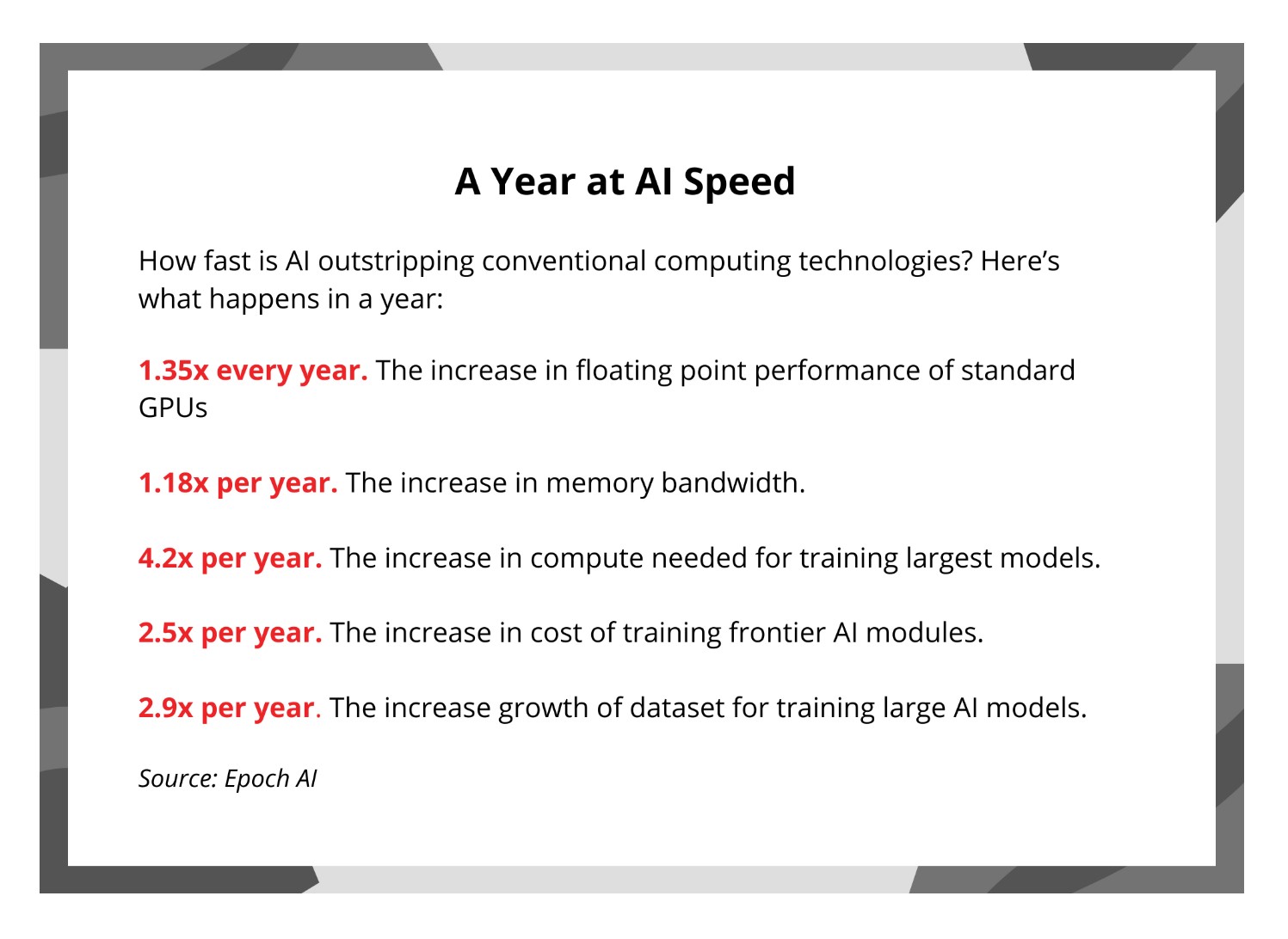
ChatGPT landed one million users within five days,1 far surpassing the pace of any previous technology. The compute requirements of training notable AI models increases 4.5x per year while training data sets mushroom by 3x per year,2 etc.
Bigger, however, comes at a price. Data center power consumption threatens to nearly triple by 2028 primarily because of AI3. Water withdrawals, meanwhile, are escalating as well: by 2027, AI data centers could need up to 6.6 billion cubic meters, or about half of what the UK uses.4 The economic and environmental toll over the long run may not be sustainable.
Conceptually it is easier to understand how larger models translate into a "better and more capable" model. The more layers or parameters the models have, contribute to the quality and accuracy of the model. Yet, can we sustain that extracted value at the same cadence by continuing the size increase? Or will the curve start to plateau at some point?
By Nick Kucharewski, Senior Vice President and General Manager, Cloud Platform Business Unit, Marvell
The rapid expansion in the size and capacity of AI workloads is significantly impacting both computing and network technologies in the modern data center. Data centers are continuously evolving to accommodate higher performance GPUs and AI accelerators (XPUs), increased memory capacities, and a push towards lower latency architectures for arranging these elements. The desire for larger clusters with shorter compute times has driven heightened focus on networking interconnects, with designers embracing state-of-the-art technologies to ensure efficient data movement and communication between the components comprising the AI cloud.
A large-scale AI cloud data center can contain hundreds of thousands, or millions, of individual links between the devices performing compute, switching, and storage functions. Inside the cloud, there is a tightly ordered fabric of high-speed interconnects: webs of copper wire and glass fiber each carrying digital signals at roughly 100 billion bits per second. Upon close inspection there is a pattern and a logical ordering to each link used for every connection in the cloud, which can be analyzed by considering the physical attributes of different types of links.
For inspiration, we can look back 80 years to the origins of modern computing, when John von Neumann posed the concept of memory hierarchy for computer architectures1. In 1945 Von Neumann proposed a smaller faster storage memory placed close to the compute circuitry, and a larger slower storage medium placed further away, to enable a system delivering both performance and scale. This concept of memory hierarchy is now pervasive, with the terms “Cache”, “DRAM”, and “Flash” part of our everyday language. In today’s AI cloud data centers, we can analyze the hierarchy of interconnects in much the same way. It is a layered structure of links, strategically utilized according to their innate physical attributes of speed, power consumption, reach, and cost.
The hierarchy of interconnects
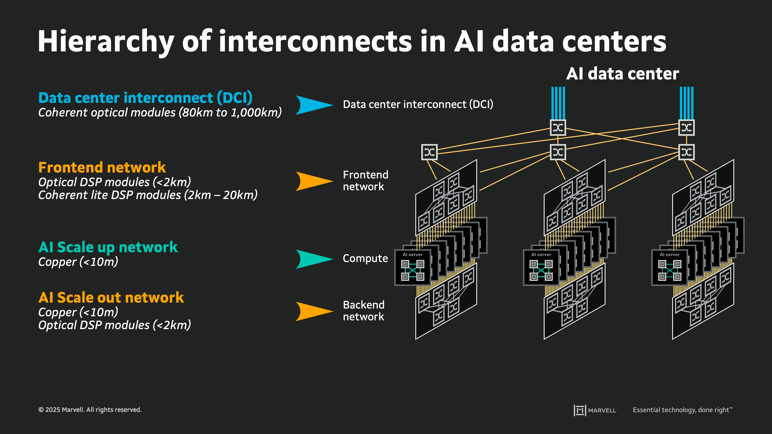
This hierarchy of interconnects provides a framework for understanding emerging interconnect technologies and to assess their potential impact in the next generation of AI data centers. Through a discussion of the basic attributes of emerging interconnect technologies in the context of the goals and aims of the AI cloud design, we can estimate how these technologies may be deployed in the coming years. By identifying the desired attributes for each use case, and the key design constraints, we can also predict when new technologies will pass the "tipping point" enabling widespread adoption in future cloud deployments.
By Kirt Zimmer, Head of Social Media Marketing, Marvell
What do you get when you combine some of the world’s leading technology analysts with incredibly smart subject matter experts? Answer: the SixFive Media video podcast. It’s must-view content for anyone interested in understanding exactly how AI technologies are evolving.
At Marvell’s recent Investor Analysts Day, company leaders were happy to chat with Patrick Moorhead, CEO and Chief Analyst at Moor Insights & Strategy, and Daniel Newman, CEO and Chief Analyst at The Futurum Group. The resulting conversations (captured on video) were enlightening:
How Custom HBM is Shaping AI Chip Technology
Fresh off Marvell’s announcement of a partnership with SK Hynix, Micron Technology and Samsung Semiconductor, Patrick and Daniel dove into the details with leaders from those organizations. The partnership centers around custom high bandwidth memory (HBM), which fits inside AI accelerators to store data close to the processors.
Custom designs alleviate the physical and thermal constraints traditionally faced by chip designers by dramatically reducing the size and power consumption of the interface and HBM base die. Marvell estimates that up to 25% of the real estate inside the chip package can be recovered via customization.
Will Chu, SVP and GM of Custom Compute and Storage at Marvell, says the company estimates that the total addressable market (TAM) for data centers in 3-4 years is $75B. Last year it was $21B. Out of that, Marvell estimates that $40-43B is for custom accelerators.
Attached to that is custom HBM, which alleviates bottlenecks for AI workloads. In Dong Kim, VP of Product Planning at Samsung Semiconductor said, “Custom HBM will be the majority portion of the market towards the 2027-28 timeframe.” As Patrick Moorhead said, “The rate of change is phenomenal.”