
By Kirt Zimmer, Head of Social Media Marketing, Marvell
What do you get when you combine some of the world’s leading technology analysts with incredibly smart subject matter experts? Answer: the SixFive Media video podcast. It’s must-view content for anyone interested in understanding exactly how AI technologies are evolving.
At Marvell’s recent Investor Analysts Day, company leaders were happy to chat with Patrick Moorhead, CEO and Chief Analyst at Moor Insights & Strategy, and Daniel Newman, CEO and Chief Analyst at The Futurum Group. The resulting conversations (captured on video) were enlightening:
How Custom HBM is Shaping AI Chip Technology
Fresh off Marvell’s announcement of a partnership with SK Hynix, Micron Technology and Samsung Semiconductor, Patrick and Daniel dove into the details with leaders from those organizations. The partnership centers around custom high bandwidth memory (HBM), which fits inside AI accelerators to store data close to the processors.
Custom designs alleviate the physical and thermal constraints traditionally faced by chip designers by dramatically reducing the size and power consumption of the interface and HBM base die. Marvell estimates that up to 25% of the real estate inside the chip package can be recovered via customization.
Will Chu, SVP and GM of Custom Compute and Storage at Marvell, says the company estimates that the total addressable market (TAM) for data centers in 3-4 years is $75B. Last year it was $21B. Out of that, Marvell estimates that $40-43B is for custom accelerators.
Attached to that is custom HBM, which alleviates bottlenecks for AI workloads. In Dong Kim, VP of Product Planning at Samsung Semiconductor said, “Custom HBM will be the majority portion of the market towards the 2027-28 timeframe.” As Patrick Moorhead said, “The rate of change is phenomenal.”
By Kirt Zimmer, Head of Social Media Marketing, Marvell

Marvell’s business is accelerated infrastructure for the AI era, which is a fast-evolving space that can occasionally confuse even the most earnest student. To help you keep up, we’ve partnered with VentureBeat to explore a multitude of content about that subject:
By Michael Kanellos, Head of Influencer Relations, Marvell
Computer architects have touted the performance and efficiency gains that can be achieved by replacing copper interconnects with optical technology in servers and processors for decades1.
With AI, it’s finally happening.
Marvell earlier this month announced that it will integrate co-packaged optics (CPO) technology into custom AI accelerators to improve the bandwidth, performance and efficiency of the chips powering AI training clusters and inference servers and opening the door to higher-performing scale-up servers.
The foundation of the offering is the Marvell 6.4Tbps 3D SiPho Engine announced in December 2023 and first demonstrated at OFC in March 2024. The 3D SiPho Engine effectively combines hundreds of components—drivers, transimpedance amplifiers, modulators, etc.—into a chiplet that itself becomes part of the XPU.
With CPO, XPUs will connect directly into an optical scale-up network, transmitting data further, faster, and with less energy per bit. LightCounting estimates that shipments of CPO-enabled ports in servers and other equipment will rise from a nominal number of shipments per year today to over 18 million by 20292.
Additionally, the bandwidth provided by CPO lets system architects think big. Instead of populating data centers with conventional servers containing four or eight XPUs, clouds can shift to systems sporting hundreds or even thousands of CPO-enhanced XPUs spread over multiple racks based around novel architectures—innovative meshes, torus networks—that can slash cost, latency and power. If supercomputers became clusters of standard servers in the 2000s, AI is shifting the pendulum back and turning servers into supercomputers again.
“It enables a huge diversity of parallelism schemes that were not possible with a smaller scale-up network domain,” wrote Dylan Patel of SemiAnalysis in a December article.
By Michael Kanellos, Head of Influencer Relations, Marvell
What happened in semis and accelerated infrastructure in 2024? Here is the recap:
1. Custom Controls the Future
Until relatively recently, computing performance was achieved by increasing transistor density à la Moore’s Law. In the future, it will be achieved through innovative design, and many of those innovative design ideas will come to market first—and mostly— through custom processors tailored to use cases, software environments and performance goals thanks to a convergence of unusual and unstoppable forces1 that quietly began years ago.
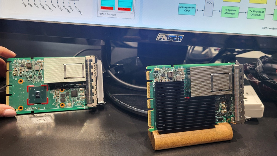
FB NIC on display at OFC
By Michael Kanellos, Head of Influencer Relations, Marvell
The idea of customizing high bandwidth memory (HBM) has only recently emerged, but expect to see it in the mainstream in just a few years.
“We strongly believe that custom HBM will be the majority portion of the market towards the ’27-28 time frame,” said In Dong Kim, vice president of product planning at Samsung Semiconductor in a video interview with the Six Five at Marvell Analyst Day earlier this month where Marvell, Micron Technology, Samsung and SK hynix announced a collaboration to accelerate the development of custom HBM solutions.
Sunny Kang, vice president of DRAM technology at SK Hynix had a similar outlook. “Usually in the DRAM industry, when we launch a new product, it takes just one or two years to be mainstream,” he said. “That means along the ‘29 timeframe, it is going to be a mainstream product in the HBM market. I’m pretty sure about that.”